101 Innovation Drive
San Jose, CA 95134
www.altera.com
TU-N2HWDV-4.0
Tutorial
Nios II Hardware Development
Subscribe
Nios II Hardware Development Tutorial
Nios II Hardware Development Tutorial May 2011 Altera Corporation
© 2011 Altera Corporation. All rights reserved. ALTERA, ARRIA, CYCLONE, HARDCOPY, MAX, MEGACORE, NIOS, QUARTUS and STRATIX are Reg. U.S. Pat.
& Tm. Off. and/or trademarks of Altera Corporation in the U.S. and other countries. All other trademarks and service marks are the property of their respective
holders as described at www.altera.com/common/legal.html. Altera warrants performance of its semiconductor products to current specifications in accordance
with Altera’s standard warranty, but reserves the right to make changes to any products and services at any time without notice. Altera assumes no responsibility or
liability arising out of the application or use of any information, product, or service described herein except as expressly agreed to in writing by Altera. Altera
customers are advised to obtain the latest version of device specifications before relying on any published information and before placing orders for products or
services.
May 2011 Altera Corporation Nios II Hardware Development Tutorial
Contents
Chapter 1. Nios II Hardware Development
Design Example . . . . . . . . . . . . . . . . . . . . . . . . . . . . . . . . . . . . . . . . . . . . . . . . . . . . . . . . . . . . . . . . . . . . . . . . . 1–1
Software and Hardware Requirements . . . . . . . . . . . . . . . . . . . . . . . . . . . . . . . . . . . . . . . . . . . . . . . . . . . . . 1–2
OpenCore Plus Evaluation . . . . . . . . . . . . . . . . . . . . . . . . . . . . . . . . . . . . . . . . . . . . . . . . . . . . . . . . . . . . . . . . 1–3
Nios II System Development Flow . . . . . . . . . . . . . . . . . . . . . . . . . . . . . . . . . . . . . . . . . . . . . . . . . . . . . . . . . 1–4
Analyzing System Requirements . . . . . . . . . . . . . . . . . . . . . . . . . . . . . . . . . . . . . . . . . . . . . . . . . . . . . . . . 1–5
Defining and Generating the System in Qsys . . . . . . . . . . . . . . . . . . . . . . . . . . . . . . . . . . . . . . . . . . . . . 1–5
Integrating the Qsys System into the Quartus II Project . . . . . . . . . . . . . . . . . . . . . . . . . . . . . . . . . . . . 1–6
Developing Software with the Nios II Software Build Tools for Eclipse . . . . . . . . . . . . . . . . . . . . . . . 1–6
Running and Debugging Software on the Target Board . . . . . . . . . . . . . . . . . . . . . . . . . . . . . . . . . . . . 1–7
Varying the Development Flow . . . . . . . . . . . . . . . . . . . . . . . . . . . . . . . . . . . . . . . . . . . . . . . . . . . . . . . . . 1–7
Refining the Software and Hardware . . . . . . . . . . . . . . . . . . . . . . . . . . . . . . . . . . . . . . . . . . . . . . . . . . 1–7
Iteratively Creating a Nios II System . . . . . . . . . . . . . . . . . . . . . . . . . . . . . . . . . . . . . . . . . . . . . . . . . . 1–7
Verifying the System with Hardware Simulation Tools . . . . . . . . . . . . . . . . . . . . . . . . . . . . . . . . . . 1–8
Creating the Design Example . . . . . . . . . . . . . . . . . . . . . . . . . . . . . . . . . . . . . . . . . . . . . . . . . . . . . . . . . . . . . 1–8
Install the Design Files . . . . . . . . . . . . . . . . . . . . . . . . . . . . . . . . . . . . . . . . . . . . . . . . . . . . . . . . . . . . . . . . . 1–8
Analyze System Requirements . . . . . . . . . . . . . . . . . . . . . . . . . . . . . . . . . . . . . . . . . . . . . . . . . . . . . . . . . . 1–9
Start the Quartus II Software and Open the Example Project . . . . . . . . . . . . . . . . . . . . . . . . . . . . . . . . 1–9
Create a New Qsys System . . . . . . . . . . . . . . . . . . . . . . . . . . . . . . . . . . . . . . . . . . . . . . . . . . . . . . . . . . . . 1–10
Define the System in Qsys . . . . . . . . . . . . . . . . . . . . . . . . . . . . . . . . . . . . . . . . . . . . . . . . . . . . . . . . . . . . . 1–11
Specify Target FPGA and Clock Settings . . . . . . . . . . . . . . . . . . . . . . . . . . . . . . . . . . . . . . . . . . . . . . 1–11
Add the On-Chip Memory . . . . . . . . . . . . . . . . . . . . . . . . . . . . . . . . . . . . . . . . . . . . . . . . . . . . . . . . . . 1–12
Add the Nios II Processor Core . . . . . . . . . . . . . . . . . . . . . . . . . . . . . . . . . . . . . . . . . . . . . . . . . . . . . . 1–14
Add the JTAG UART . . . . . . . . . . . . . . . . . . . . . . . . . . . . . . . . . . . . . . . . . . . . . . . . . . . . . . . . . . . . . . 1–17
Add the Interval Timer . . . . . . . . . . . . . . . . . . . . . . . . . . . . . . . . . . . . . . . . . . . . . . . . . . . . . . . . . . . . . 1–18
Add the System ID Peripheral . . . . . . . . . . . . . . . . . . . . . . . . . . . . . . . . . . . . . . . . . . . . . . . . . . . . . . . 1–19
Add the PIO . . . . . . . . . . . . . . . . . . . . . . . . . . . . . . . . . . . . . . . . . . . . . . . . . . . . . . . . . . . . . . . . . . . . . . 1–20
Specify Base Addresses and Interrupt Request Priorities . . . . . . . . . . . . . . . . . . . . . . . . . . . . . . . . 1–22
Generate the Qsys System . . . . . . . . . . . . . . . . . . . . . . . . . . . . . . . . . . . . . . . . . . . . . . . . . . . . . . . . . . 1–23
Integrate the Qsys System into the Quartus II Project . . . . . . . . . . . . . . . . . . . . . . . . . . . . . . . . . . . . . 1–24
Instantiate the Qsys System Module in the Quartus II Project . . . . . . . . . . . . . . . . . . . . . . . . . . . . 1–25
Add IP Variation File . . . . . . . . . . . . . . . . . . . . . . . . . . . . . . . . . . . . . . . . . . . . . . . . . . . . . . . . . . . . . . 1–26
Assign FPGA Device and Pin Locations . . . . . . . . . . . . . . . . . . . . . . . . . . . . . . . . . . . . . . . . . . . . . . 1–26
Compile the Quartus II Project and Verify Timing . . . . . . . . . . . . . . . . . . . . . . . . . . . . . . . . . . . . . 1–29
Download Hardware Design to Target FPGA . . . . . . . . . . . . . . . . . . . . . . . . . . . . . . . . . . . . . . . . . . . . 1–31
Develop Software Using the Nios II SBT for Eclipse . . . . . . . . . . . . . . . . . . . . . . . . . . . . . . . . . . . . . . . 1–32
Create a New Nios II Application and BSP from Template . . . . . . . . . . . . . . . . . . . . . . . . . . . . . . 1–32
Compile the Project . . . . . . . . . . . . . . . . . . . . . . . . . . . . . . . . . . . . . . . . . . . . . . . . . . . . . . . . . . . . . . . . 1–34
Run the Program on Target Hardware . . . . . . . . . . . . . . . . . . . . . . . . . . . . . . . . . . . . . . . . . . . . . . . . . . 1–35
Taking the Next Step . . . . . . . . . . . . . . . . . . . . . . . . . . . . . . . . . . . . . . . . . . . . . . . . . . . . . . . . . . . . . . . . . . . . 1–36
Additional Information
Document Revision History . . . . . . . . . . . . . . . . . . . . . . . . . . . . . . . . . . . . . . . . . . . . . . . . . . . . . . . . . . . Info–1
How to Contact Altera . . . . . . . . . . . . . . . . . . . . . . . . . . . . . . . . . . . . . . . . . . . . . . . . . . . . . . . . . . . . . . . . Info–1
Typographic Conventions . . . . . . . . . . . . . . . . . . . . . . . . . . . . . . . . . . . . . . . . . . . . . . . . . . . . . . . . . . . . . Info–2
iv Contents
Nios II Hardware Development Tutorial May 2011 Altera Corporation
May 2011 Altera Corporation Nios II Hardware Development Tutorial
1. Nios II Hardware Development
This tutorial introduces you to the system development flow for the Nios® II
processor. Using the Quartus® II software and the Nios II Embedded Design Suite
(EDS), you build a Nios II hardware system design and create a software program
that runs on the Nios II system and interfaces with components on Altera®
development boards. The tutorial is a good starting point if you are new to the Nios II
processor or the general concept of building embedded systems in FPGAs.
Building embedded systems in FPGAs involves system requirements analysis,
hardware design tasks, and software design tasks. This tutorial guides you through
the basics of each topic, with special focus on the hardware design steps. Where
appropriate, the tutorial refers you to further documentation for greater detail.
f If you are interested only in software development for the Nios II processor, refer to
the tutorial in the Getting Started with the Graphical User Interface chapter of the Nios II
Software Developer’s Handbook.
When you complete this tutorial, you will understand the Nios II system
development flow, and you will be able to create your own custom Nios II system.
Design Example
The design example you build in this tutorial demonstrates a small Nios II system for
control applications, that displays character I/O output and blinks LEDs in a binary
counting pattern. This Nios II system can also communicate with a host computer,
allowing the host computer to control logic inside the FPGA.
The example Nios II system contains the following components:
■ Nios II/s processor core
■ On-chip memory
■ Timer
■ JTAG UART
■ 8-bit parallel I/O (PIO) pins to control the LEDs
■ System identification component
1–2 Chapter 1: Nios II Hardware Development
Software and Hardware Requirements
Nios II Hardware Development Tutorial May 2011 Altera Corporation
Figure 1–1 is a block diagram showing the relationship among the host computer, the
target board, the FPGA, and the Nios II system.
As shown in Figure 1–1, other logic can exist within the FPGA alongside the Nios II
system. In fact, most FPGA designs with a Nios II system also include other logic. A
Nios II system can interact with other on-chip logic, depending on the needs of the
overall system. For the sake of simplicity, the design example in this tutorial does not
include other logic in the FPGA.
Software and Hardware Requirements
This tutorial requires you to have the following software:
■ Altera Quartus II software version 11.0 or later—The software must be installed on
a Windows or Linux computer that meets the Quartus II minimum requirements.
f For system requirements and installation instructions, refer to Altera
Software Installation and Licensing.
■ Nios II EDS version 11.0 or later.
■ Design files for the design example—A hyperlink to the design files appears next
to this document on the Literature: Nios II Processor page of the Altera website.
Figure 1–1. Tutorial Design Example
Nios II System
Character
I/O
Instr
Data
Debug
control 8
Other logic
Altera FPGA
Target Board
LED5
LED0
LED1
LED2
LED3
LED4
LED6
LED7
VCC
Clock
oscillator
System interconnect fabric
Timer
PIO
System
ID
On-chip
RAM
Nios II/s
core
JTAG
UART
JTAG controller
10-pin
JTAG
header
Chapter 1: Nios II Hardware Development 1–3
OpenCore Plus Evaluation
May 2011 Altera Corporation Nios II Hardware Development Tutorial
You can build the design example in this tutorial with any Altera development board
or your own custom board that meets the following requirements:
■ The board must have an Altera Stratix® series, Cyclone® series, or Arria® series
FPGA.
■ The FPGA must contain a minimum of 2500 logic elements (LE) or adaptive lookup
tables (ALUT).
■ The FPGA must contain a minimum of 50 M4K or M9K memory blocks.
■ An oscillator must drive a constant clock frequency to an FPGA pin. The
maximum frequency limit depends on the speed grade of the FPGA. Frequencies
of 50 MHz or less should work for most boards; higher frequencies might work.
■ FPGA I/O pins can optionally connect to eight or fewer LEDs to provide a visual
indicator of processor activity.
■ The board must have a JTAG connection to the FPGA that provides a
programming interface and communication link to the Nios II system. This
connection can be a dedicated 10-pin JTAG header for an Altera USB-Blaster™
download cable (revision B or higher) or a USB connection with USB-Blaster
circuitry embedded on the board.
1 To complete this tutorial, you must refer to the documentation for your board that
describes clock frequencies and pinouts. For Altera development boards, you can find
this information in the associated reference manual.
f For information about Altera development kits and development boards, refer to the
Literature: Development Kits page of the Altera website.
OpenCore Plus Evaluation
You can perform this tutorial on hardware without a license. With Altera's free
OpenCore Plus evaluation feature, you can perform the following actions:
■ Simulate the behavior of a Nios II processor within your system
■ Verify the functionality of your design
■ Evaluate the size and speed of your design quickly and easily
■ Generate time-limited device programming files for designs that include Nios II
processors
■ Program a device and verify your design in hardware
You need to purchase a license for the Nios II processor only when you are completely
satisfied with its functionality and performance, and want to use your design in
production.
f For more information about OpenCore Plus, refer to OpenCore Plus Evaluation of
Megafunctions.
1–4 Chapter 1: Nios II Hardware Development
Nios II System Development Flow
Nios II Hardware Development Tutorial May 2011 Altera Corporation
Nios II System Development Flow
This section discusses the complete design flow for creating a Nios II system and
prototyping it on a target board. Figure 1–2 shows the Nios II system development
flow.
The Nios II development flow consists of three types of development: hardware
design steps, software design steps, and system design steps, involving both
hardware and software. For simpler Nios II systems, one person might perform all
steps. For more complex systems, separate hardware and software designers might be
responsible for different steps. System design steps involve both the hardware and
software, and might require input from both sides. In the case of separate hardware
and software teams, it is important to know exactly what files and information must
be passed between teams at the points of intersection in the design flow.
The design steps in this tutorial focus on hardware development, and provide only a
simple introduction to software development.
f After completing this tutorial, refer to the Nios II Software Developer’s Handbook,
especially the tutorial in the Getting Started with the Graphical User Interface chapter, for
more information about the software development process. The handbook is a
complete reference for developing software for the Nios II processor.
Figure 1–2. Nios II System Development Flow
Altera
hardware
abstraction
layer
and
peripheral
drivers
Define and generate
system in Qsys
Analyze system
requirements
User C/C++
application
code and
custom
libraries
Custom
instruction
and
custom
peripheral
logic
Custom
hardware
modules
Nios II
cores
and
standard
peripherals
Integrate Qsys system
into Quartus II project
Develop software with
the Nios II Software
Build Tools for Eclipse
Assign pin locations,
timing requirements
and other design constraints
Download FPGA design
to target board
Compile hardware design
for target board
Run and debug software
on target board
Refine software
and hardware
Download software executable
to Nios II system on target board
Chapter 1: Nios II Hardware Development 1–5
Nios II System Development Flow
May 2011 Altera Corporation Nios II Hardware Development Tutorial
Analyzing System Requirements
The development flow begins with predesign activity which includes an analysis of
the application requirements, such as the following questions:
■ What computational performance does the application require?
■ How much bandwidth or throughput does the application require?
■ What types of interfaces does the application require?
■ Does the application require multithreaded software?
Based on the answers to these questions, you can determine the concrete system
requirements, such as:
■ Which Nios II processor core to use: smaller or faster.
■ What components the design requires and how many of each kind.
■ Which real-time operating system (RTOS) to use, if any.
■ Where hardware acceleration logic can dramatically improve system performance.
For example:
■ Could adding a DMA component eliminate wasted processor cycles copying
data?
■ Could a custom instruction replace the critical loop of a DSP algorithm?
Analyzing these topics involve both the hardware and software teams.
Defining and Generating the System in Qsys
After analyzing the system hardware requirements, you use Qsys to specify the
Nios II processor core(s), memory, and other components your system requires. Qsys
automatically generates the interconnect logic to integrate the components in the
hardware system.
You can select from a list of standard processor cores and components provided with
the Nios II EDS. You can also add your own custom hardware to accelerate system
performance. You can add custom instruction logic to the Nios II core which
accelerates CPU performance, or you can add a custom component which offloads
tasks from the CPU. This tutorial covers adding standard processor and component
cores, and does not cover adding custom logic to the system.
The primary outputs of Qsys are the following file types:
■ Qsys Design File (.qsys)—Contains the hardware contents of the Qsys system.
■ SOPC Information File (.sopcinfo)—Contains a description of the contents of the
.qsys file in Extensible Markup Language File (.xml) format. The Nios II EDS uses
the .sopcinfo file to create software for the target hardware.
■ Hardware description language (HDL) files—Are the hardware design files that
describe the Qsys system. The Quartus II software uses the HDL files to compile
the overall FPGA design into an SRAM Object File (.sof).
1–6 Chapter 1: Nios II Hardware Development
Nios II System Development Flow
Nios II Hardware Development Tutorial May 2011 Altera Corporation
f For more information about the following topics, refer to the related documentation:
■ For Nios II processor cores, refer to the Nios II Processor Reference Handbook.
■ For Qsys and developing custom components, refer to the System Design with Qsys
section of Volume 1: Design and Synthesis of the Quartus II Handbook.
■ For custom instructions, refer to the Nios II Custom Instruction User Guide.
Integrating the Qsys System into the Quartus II Project
After generating the Nios II system using Qsys, you integrate it into the Quartus II
project. Using the Quartus II software, you perform all tasks required to create the
final FPGA hardware design.
As shown in Figure 1–1 on page 1–2, most FPGA designs include logic outside the
Nios II system. You can integrate your own custom hardware modules into the FPGA
design, or you can integrate other ready-made intellectual property (IP) design
modules available from Altera or third party IP providers. This tutorial does not cover
adding other logic outside the Nios II system.
Using the Quartus II software, you also assign pin locations for I/O signals, specify
timing requirements, and apply other design constraints. Finally, you compile the
Quartus II project to produce a .sof to configure the FPGA.
You download the .sof to the FPGA on the target board using an Altera download
cable, such as the USB-Blaster. After configuration, the FPGA behaves as specified by
the hardware design, which in this case is a Nios II processor system.
f For further information about using the Quartus II software, refer to Introduction to the
Quartus II Software, the Quartus II Handbook, and the Quartus II Software Interactive
Tutorial in the Training Courses section of the Altera website.
Developing Software with the Nios II Software Build Tools for Eclipse
Using the Nios II Software Build Tools (SBT) for Eclipse™, you perform all software
development tasks for your Nios II processor system. After you generate the system
with Qsys, you can begin designing your C/C++ application code immediately with
the Nios II SBT for Eclipse. Altera provides component drivers and a hardware
abstraction layer (HAL) which allows you to write Nios II programs quickly and
independently of the low-level hardware details. In addition to your application code,
you can design and reuse custom libraries in your Nios II SBT for Eclipse projects.
To create a new Nios II C/C++ application project, the Nios II SBT for Eclipse uses
information from the .sopcinfo file. You also need the .sof file to configure the FPGA
before running and debugging the application project on target hardware.
The Nios II SBT for Eclipse can produce several outputs, listed below. Not all projects
require all of these outputs.
■ system.h file—Defines symbols for referencing the hardware in the system. The
Nios II SBT for Eclipse automatically create this file when you create a new board
support package (BSP).
■ Executable and Linking Format File (.elf)—Is the result of compiling a C/C++
application project, that you can download directly to the Nios II processor.
Chapter 1: Nios II Hardware Development 1–7
Nios II System Development Flow
May 2011 Altera Corporation Nios II Hardware Development Tutorial
■ Hexadecimal (Intel-Format) File (.hex)—Contains initialization information for
on-chip memories. The Nios II SBT for Eclipse generate these initialization files for
on-chip memories that support initialization of contents.
■ Flash memory programming data—Is boot code and other arbitrary data you
might write to flash memory. The Nios II SBT for Eclipse includes a flash
programmer, which allows you to write your program to flash memory. The flash
programmer adds appropriate boot code to allow your program to boot from flash
memory. You can also use the flash programmer to write arbitrary data to flash
memory.
This tutorial focuses on downloading only the .elf directly to the Nios II system.
f For extensive information about developing software for the Nios II processor, refer to
the Nios II Software Developer's Handbook.
Running and Debugging Software on the Target Board
The Nios II SBT for Eclipse provides complete facilities for downloading software to a
target board, and running or debugging the program on hardware. The Nios II SBT
for Eclipse debugger allows you to start and stop the processor, step through code, set
breakpoints, and analyze variables as the program executes.
f For information about running and debugging Nios II programs, refer to the tutorial
in the Getting Started with the Graphical User Interface chapter of the Nios II Software
Developer’s Handbook.
Varying the Development Flow
The development flow is not strictly linear. This section describes common variations.
Refining the Software and Hardware
After running software on the target board, you might discover that the Nios II
system requires higher performance. In this case, you can return to software design
steps to make improvements to the software algorithm. Alternatively, you can return
to hardware design steps to add acceleration logic. If the system performs multiple
mutually exclusive tasks, you might even decide to use two (or more) Nios II
processors that divide the workload and improve the performance of each individual
processor.
Iteratively Creating a Nios II System
A common technique for building a complex Nios II system is to start with a simpler
Qsys system, and iteratively add to it. At each iteration, you can verify that the system
performs as expected. You might choose to verify the fundamental components of a
system, such as the processor, memory, and communication channels, before adding
more complex components. When developing a custom component or a custom
instruction, first integrate the custom logic into a minimal system to verify that it
works as expected; later you can integrate the custom logic into a more complex
system.
1–8 Chapter 1: Nios II Hardware Development
Creating the Design Example
Nios II Hardware Development Tutorial May 2011 Altera Corporation
f Altera provides several working Nios II reference designs which you can use as a
starting point for your own designs. After installing the Nios II EDS, refer to the
<Nios II EDS install path>/examples/verilog or the <Nios II EDS install path>/
examples/vhdl directory. Demonstration applications are also available in newer
development kit installations.
Verifying the System with Hardware Simulation Tools
You can perform hardware simulation of software executing on the Nios II system,
using tools such as the ModelSim® RTL simulator. Hardware simulation is useful to
meet certain needs, including the following cases:
■ To verify the cycle-accurate performance of a Nios II system before target
hardware is available.
■ To verify the functionality of a custom component or a Nios II custom instruction
before trying it on hardware.
A hardware simulation step is not shown in Figure 1–2 on page 1–4. If you are
building a Nios II system based on the standard components provided with the
Nios II EDS, the easiest way to verify functionality is to download the hardware and
software directly to a development board.
f For information about performing hardware simulation for Nios II system, refer to
Simulating Nios II Embedded Processor Designs.
Creating the Design Example
This section guides you through the Nios II development flow to create a working
design example. You perform the following steps:
1. “Install the Design Files” on page 1–8.
2. “Analyze System Requirements” on page 1–9.
3. “Start the Quartus II Software and Open the Example Project” on page 1–9.
4. “Create a New Qsys System” on page 1–10.
5. “Define the System in Qsys” on page 1–11.
6. “Integrate the Qsys System into the Quartus II Project” on page 1–24.
7. “Download Hardware Design to Target FPGA” on page 1–31.
8. “Develop Software Using the Nios II SBT for Eclipse” on page 1–32.
9. “Run the Program on Target Hardware” on page 1–35.
Install the Design Files
Before you proceed, you must install the Quartus II software and the Nios II EDS. You
must also download tutorial design files from the Altera web site. The design files
provide a ready-made Quartus II project to use as a starting point.
f The design files appear next to this document on the Literature: Nios II Processor
page of the Altera website.
Chapter 1: Nios II Hardware Development 1–9
Creating the Design Example
May 2011 Altera Corporation Nios II Hardware Development Tutorial
Perform the following steps to set up the design environment:
1. Locate the zipped design files on the Altera web site.
2. Unzip the contents of the zip file to a directory on your computer. Do not use
spaces in the directory path name.
The remainder of this tutorial refers to this directory as the <design files directory>.
Analyze System Requirements
This section describes the system requirements for the tutorial design example. The
design example has the following goals:
■ Demonstrate a simple Nios II processor system that you can use for control
applications.
■ Build a practical, real-world system, while providing an educational experience.
■ Demonstrate the most common and effective techniques to build practical, custom
Nios II systems.
■ Build a Nios II system that works on any board with an Altera FPGA. The entire
system must use only on-chip resources, and not rely on the target board.
■ The design should conserve on-chip logic and memory resources so it can fit in a
wide range of target FPGAs.
These goals lead to the following design decisions:
■ The Nios II system uses only the following inputs and outputs:
■ One clock input, which can be any constant frequency.
■ Eight optional outputs to control LEDs on the target board.
■ The design uses the following components:
■ Nios II/s core with 2 KB of instruction cache
■ 20 KB of on-chip memory
■ Timer
■ JTAG UART
■ Eight output-only parallel I/O (PIO) pins
■ System ID component
f For more information about these and other components, refer to the Embedded
Peripherals IP User Guide.
Start the Quartus II Software and Open the Example Project
To start, you open the Quartus II project for the tutorial design example. This
Quartus II project serves as an easy starting point for the Nios II development flow.
The Quartus II project contains all settings and design files required to create the .sof.
1–10 Chapter 1: Nios II Hardware Development
Creating the Design Example
Nios II Hardware Development Tutorial May 2011 Altera Corporation
To open the Quartus II project, perform the following steps:
1. Start the Quartus II software.
On Windows computers, click Start, point to Programs, Altera, Quartus II
<version>, and then click Quartus II <version>. On Linux computers, type quartus
at a shell command prompt, assuming the Quartus II program directory is in the
search path.
2. Click Open Existing Project on the splash screen, or, on the File menu, click Open
Project. The Open Project dialog box appears.
3. Browse to the <design files directory>.
4. Select the file nios2_quartus2_project.qpf and click Open. The project opens.
5. To display the Block Diagram File (.bdf) nios2_quartus2_project.bdf (Figure 1–3),
perform the following steps:
a. On the File menu, click Open. The Open dialog box appears.
b. Browse to the <design files directory>.
c. Select nios2_quartus2_project.bdf and click Open.
Figure 1–3 shows the nios2_quartus2_project.bdf file.
The .bdf contains an input pin for the clock input and eight output pins to drive LEDs
on the board. Next, you create a new Qsys system, which you ultimately connect to
these pins.
Create a New Qsys System
You use Qsys to generate the Nios II processor system, adding the desired
components, and configuring how they connect together. To create a new Qsys
system, click Qsys on the Tools menu in the Quartus II software. Qsys starts and
displays the System Contents tab.
Figure 1–3. Design Example Block Diagram File
Chapter 1: Nios II Hardware Development 1–11
Creating the Design Example
May 2011 Altera Corporation Nios II Hardware Development Tutorial
Figure 1–4 shows the Qsys GUI in its initial state.
Define the System in Qsys
You use Qsys to define the hardware characteristics of the Nios II system, such as
which Nios II core to use, and what components to include in the system. Qsys does
not define software behavior, such as where in memory to store instructions or where
to send the stderr character stream.
In this section, you perform the following steps:
1. Specify target FPGA and clock settings.
2. Add the Nios II core, on-chip memory, and other components.
3. Specify base addresses and interrupt request (IRQ) priorities.
4. Generate the Qsys system.
The Qsys design process does not need to be linear. The design steps in this tutorial
are presented in the most straightforward order for a new user to understand.
However, you can perform Qsys design steps in a different order.
Specify Target FPGA and Clock Settings
The Clock Settings and the Project Settings tabs specify the Qsys system's
relationship to other devices in the system.
Figure 1–4. Qsys GUI
1–12 Chapter 1: Nios II Hardware Development
Creating the Design Example
Nios II Hardware Development Tutorial May 2011 Altera Corporation
Perform the following steps:
1. On the Project Settings tab, select the Device Family that matches the Altera
FPGA you are targeting.
1 If a warning appears stating the selected device family does not match the
Quartus project settings, ignore the warning. You specify the device in the
Quartus project settings later in this tutorial.
2. In the documentation for your board, look up the clock frequency of the oscillator
that drives the FPGA.
f For Altera development board reference manuals, refer to the Literature:
Development Kits page of the Altera website.
3. On the Clock Settings tab, double-click the clock frequency in the MHz column
for clk_0. clk_0 is the default clock input name for the Qsys system. The
frequency you specify for clk_0 must match the oscillator that drives the FPGA.
4. Type the clock frequency and press Enter.
Next, you begin to add hardware components to the Qsys system. As you add each
component, you configure it appropriately to match the design specifications.
Add the On-Chip Memory
Processor systems require at least one memory for data and instructions. This design
example uses one 20 KB on-chip memory for both data and instructions. To add the
memory, perform the following steps:
1. On the Component Library tab (to the left of the System Contents tab), expand
Memories and Memory Controllers, expand On-Chip, and then click On-Chip
Memory (RAM or ROM).
2. Click Add. The On-Chip Memory (RAM or ROM) parameter editor appears.
Figure 1–5 shows the GUI.
3. In the Block type list, select Auto.
4. In the Total memory size box, type 20480 to specify a memory size of 20 KB.
1 Do not change any of the other default settings.
Chapter 1: Nios II Hardware Development 1–13
Creating the Design Example
May 2011 Altera Corporation Nios II Hardware Development Tutorial
Figure 1–5 shows the On-Chip Memory (RAM or ROM) parameter editor.
5. Click Finish. You return to Qsys.
6. Click the System Contents tab. An instance of the on-chip memory appears in the
system contents table.
1 For more information about on-chip memory, you can click Documentation in the
On-Chip Memory (RAM or ROM) parameter editor. This documentation feature is
available in the parameter editor for each component.
7. In the Name column of the system contents table, right-click the on-chip memory
and click Rename.
8. Type onchip_mem and press Enter.
Figure 1–5. On-Chip Memory Parameter Editor
1–14 Chapter 1: Nios II Hardware Development
Creating the Design Example
Nios II Hardware Development Tutorial May 2011 Altera Corporation
1 You must type these tutorial component names exactly as specified. Otherwise, the
tutorial programs written for this Nios II system fail in later steps. In general, it is a
good habit to give descriptive names to hardware components. Nios II programs use
these symbolic names to access the component hardware. Therefore, your choice of
component names can make Nios II programs easier to read and understand.
Add the Nios II Processor Core
In this section you add the Nios II/s core and configure it to use 2 KB of on-chip
instruction cache memory. For educational purposes, the tutorial design example uses
the Nios II/s (standard) core, which provides a balanced trade-off between
performance and resource utilization. In reality, the Nios II/s core is more powerful
than necessary for most simple control applications.
Perform the following steps to add a Nios II/s core to the system:
1. On the Component Library tab, expand Processors, and then click Nios II
Processor.
2. Click Add. The Nios II Processor parameter editor appears, displaying the Core
Nios II tab. Figure 1–6 shows the GUI.
3. Under Select a Nios II core, select Nios II/s.
4. In the Hardware multiplication type list, select None.
5. Turn off Hardware divide.
6. Click Finish. You return to the Qsys System Contents tab, and an instance of the
Nios II core appears in the system contents table. Ignore the exception and reset
vector error messages. You resolve these errors in steps 13 and 14.
7. In the Name column, right-click the Nios II processor and click Rename.
8. Type cpu and press Enter.
9. In the Connections column, connect the clk port of the clk_0 clock source to both
the clk1 port of the on-chip memory and the clk port of the Nios II processor by
clicking the hollow dots on the connection line. The dots become solid indicating
the ports are connected.
10. Connect the clk_reset port of the clk_0 clock source to both the reset1 port of the
on-chip memory and the reset_n port of the Nios II processor.
11. Connect the s1 port of the on-chip memory to both the data_master port and
instruction_master port of the Nios II processor.
12. Double-click the Nios II processor row of the system contents table to reopen the
Nios II Processor parameter editor.
13. Under Reset Vector, select onchip_mem.s1 in the Reset vector memory list and
type 0x0 in the Reset vector offset box.
14. Under Exception Vector, select onchip_mem.s1 in the Exception vector memory
list and type 0x20 in the Exception vector offset box.
Chapter 1: Nios II Hardware Development 1–15
Creating the Design Example
May 2011 Altera Corporation Nios II Hardware Development Tutorial
Figure 1–6 shows the Core Nios II tab of the Nios II Processor parameter editor.
15. Click the Caches and Memory Interfaces tab. Figure 1–7 shows the GUI.
16. In the Instruction cache list, select 2 Kbytes.
17. In the Burst transfers list, select Disable.
18. In the Number of tightly coupled instruction master port(s) list, select None.
Figure 1–6. Nios II Parameter Editor – Core Nios II Tab
1–16 Chapter 1: Nios II Hardware Development
Creating the Design Example
Nios II Hardware Development Tutorial May 2011 Altera Corporation
Figure 1–7 shows the Caches and Memory Interfaces tab of the Nios II Processor
parameter editor.
1 Do not change any settings on the Advanced Features, MMU and MPU Settings,
JTAG Debug Module, or Custom Instruction tabs.
19. Click Finish. You return to the Qsys System Contents tab.
f For more information about configuring the Nios II core, refer to the Instantiating the
Nios II Processor in Qsys chapter of the Nios II Processor Reference Handbook.
f For more information about connecting memory to Nios II systems, refer to the System
Design with Qsys section of Volume 1: Design and Synthesis of the Quartus II Handbook.
Figure 1–7. Nios II Parameter Editor – Caches and Memory Interfaces Tab
Chapter 1: Nios II Hardware Development 1–17
Creating the Design Example
May 2011 Altera Corporation Nios II Hardware Development Tutorial
Add the JTAG UART
The JTAG UART provides a convenient way to communicate character data with the
Nios II processor through the USB-Blaster download cable. Perform the following
steps to add the JTAG UART:
1. On the Component Library tab, expand Interface Protocols, expand Serial, and
then click JTAG UART.
2. Click Add. The JTAG UART parameter editor appears.
1 Do not change the default settings.
Figure 1–8 shows the JTAG UART parameter editor.
3. Click Finish. You return to the Qsys System Contents tab, and an instance of the
JTAG UART appears in the system contents table.
4. In the Name column, right-click the JTAG UART and click Rename.
5. Type jtag_uart and press Enter.
6. Connect the clk port of the clk_0 clock source to the clk port of the JTAG UART.
Figure 1–8. JTAG UART Parameter Editor
1–18 Chapter 1: Nios II Hardware Development
Creating the Design Example
Nios II Hardware Development Tutorial May 2011 Altera Corporation
7. Connect the clk_reset port of the clk_0 clock source to the reset port of the JTAG
UART.
8. Connect the data_master port of the Nios II processor to the avalan_jtag_slave
port of the JTAG UART.
1 The instruction_master port of the Nios II processor does not connect to the JTAG
UART because the JTAG UART is not a memory device and cannot send instructions
to the Nios II processor.
f For more information about the JTAG UART, refer to the JTAG UART Core chapter in
the Embedded Peripherals IP User Guide.
Add the Interval Timer
Most control systems use a timer component to enable precise calculation of time. To
provide a periodic system clock tick, the Nios II HAL requires a timer.
Perform the following steps to add the timer:
1. On the Component Library tab, expand Peripherals, expand Microcontroller
Peripherals, and then click Interval Timer.
2. Click Add. The Interval Timer parameter editor appears. Figure 1–9 shows the
GUI.
3. In the Presets list, select Full-featured.
1 Do not change any of the other default settings.
Chapter 1: Nios II Hardware Development 1–19
Creating the Design Example
May 2011 Altera Corporation Nios II Hardware Development Tutorial
Figure 1–9 shows the Interval Timer parameter editor.
4. Click Finish. You return to the Qsys System Contents tab, and an instance of the
interval timer appears in the system contents table.
5. In the Name column, right-click the interval timer and click Rename.
6. Type sys_clk_timer and press Enter.
7. Connect the clk port of the clk_0 clock source to the clk port of the interval timer.
8. Connect the clk_reset port of the clk_0 clock source to the reset port of the
interval timer.
9. Connect the data_master port of the Nios II processor to the s1 port of the interval
timer.
f For more information about the timer, refer to the Timer Core chapter in the Embedded
Peripherals IP User Guide.
Add the System ID Peripheral
The system ID peripheral safeguards against accidentally downloading software
compiled for a different Nios II system. If the system includes the system ID
peripheral, the Nios II SBT for Eclipse can prevent you from downloading programs
compiled for a different system.
Figure 1–9. Interval Timer Parameter Editor
1–20 Chapter 1: Nios II Hardware Development
Creating the Design Example
Nios II Hardware Development Tutorial May 2011 Altera Corporation
Perform the following steps to add the system ID peripheral:
1. On the Component Library tab, expand Peripherals, expand Debug and
Performance, and then click System ID Peripheral.
2. Click Add. The System ID Peripheral parameter editor appears.
1 Do not change the default setting.
Figure 1–10 shows the System ID Peripheral parameter editor.
3. Click Finish. You return to the Qsys System Contents tab, and an instance of the
system ID peripheral appears in the system contents table.
4. In the Name column, right-click the system ID peripheral and click Rename.
5. Type sysid and press Enter.
6. Connect the clk port of the clk_0 clock source to the clk port of the system ID
peripheral.
7. Connect the clk_reset port of the clk_0 clock source to the reset port of the
system ID peripheral.
8. Connect the data_master port of the Nios II processor to the control_slave port
of the system ID peripheral.
f For more information about the system ID peripheral, refer to the System ID Core
chapter in the Embedded Peripherals IP User Guide.
Add the PIO
PIO signals provide an easy method for Nios II processor systems to receive input
stimuli and drive output signals. Complex control applications might use hundreds of
PIO signals which the Nios II processor can monitor. This design example uses eight
PIO signals to drive LEDs on the board.
Perform the following steps to add the PIO. Perform these steps even if your target
board doesn't have LEDs.
Figure 1–10. System ID Peripheral Parameter Editor
Chapter 1: Nios II Hardware Development 1–21
Creating the Design Example
May 2011 Altera Corporation Nios II Hardware Development Tutorial
1. On the Component Library tab, expand Peripherals, expand Microcontroller
Peripherals, and then click PIO (Parallel I/O).
2. Click Add. The PIO (Parallel I/O) parameter editor appears. Figure 1–11 shows
the GUI.
1 Do not change the default settings. The parameter editor defaults to an 8-bit outputonly
PIO, which exactly matches the needs for the design example.
Figure 1–11 shows the PIO (Parallel I/O) parameter editor.
3. Click Finish. You return to the Qsys System Contents tab, and an instance of the
PIO appears in the system contents table.
4. In the Name column, right-click the PIO and click Rename.
5. Type led_pio and press Enter.
6. Connect the clk port of the clk_0 clock source to the clk port of the PIO.
Figure 1–11. PIO Parameter Editor
1–22 Chapter 1: Nios II Hardware Development
Creating the Design Example
Nios II Hardware Development Tutorial May 2011 Altera Corporation
7. Connect the clk_reset port of the clk_0 clock source to the reset port of the PIO.
8. Connect the data_master port of the Nios II processor to the s1 port of the PIO.
9. In the external_connection row, click Click to export in the Export column to
export the PIO ports.
f For more information about the PIO, refer to the PIO Core chapter in the Embedded
Peripherals IP User Guide.
Specify Base Addresses and Interrupt Request Priorities
At this point, you have added all the necessary hardware components to the system.
Now you must specify how the components interact to form a system. In this section,
you assign base addresses for each slave component, and assign interrupt request
(IRQ) priorities for the JTAG UART and the interval timer.
Qsys provides the Assign Base Addresses command which makes assigning
component base addresses easy. For many systems, including this design example,
Assign Base Addresses is adequate. However, you can adjust the base addresses to
suit your needs. Below are some guidelines for assigning base addresses:
■ Nios II processor cores can address a 31-bit address span. You must assign base
address between 0x00000000 and 0x7FFFFFFF.
■ Nios II programs use symbolic constants to refer to addresses. Do not worry about
choosing address values that are easy to remember.
■ Address values that differentiate components with only a one-bit address
difference produce more efficient hardware. Do not worry about compacting all
base addresses into the smallest possible address range, because this can create
less efficient hardware.
■ Qsys does not attempt to align separate memory components in a contiguous
memory range. For example, if you want an on-chip RAM and an off-chip RAM to
be addressable as one contiguous memory range, you must explicitly assign base
addresses.
Qsys also provides an Assign Interrupt Numbers command which connects IRQ
signals to produce valid hardware results. However, assigning IRQs effectively
requires an understanding of how software responds to them. Because Qsys does not
know the software behavior, Qsys cannot make educated guesses about the best IRQ
assignment.
The Nios II HAL interprets low IRQ values as higher priority. The timer component
must have the highest IRQ priority to maintain the accuracy of the system clock tick.
To assign appropriate base addresses and IRQs, perform the following steps:
1. On the System menu, click Assign Base Addresses to make Qsys assign functional
base addresses to each component in the system. Values in the Base and End
columns might change, reflecting the addresses that Qsys reassigned.
2. In the IRQ column, connect the Nios II processor to the JTAG UART and interval
timer.
3. Click the IRQ value for the jtag_uart component to select it.
4. Type 16 and press Enter to assign a new IRQ value.
Chapter 1: Nios II Hardware Development 1–23
Creating the Design Example
May 2011 Altera Corporation Nios II Hardware Development Tutorial
5. Click the IRQ value for the sys_clk_timer component to select it.
6. Type 1 and press Enter to assign a new IRQ value.
Figure 1–12 shows the Qsys System Contents tab with the complete system.
Generate the Qsys System
You are now ready to generate the Qsys system. Perform the following steps:
1. Click the Generation tab.
2. Select None in both the Create simulation model and Create testbench Qsys
system lists. Because this tutorial does not cover the hardware simulation flow,
you can select these settings to shorten generation time.
3. Click Generate. The Save changes? dialog box appears, prompting you to save
your design.
Figure 1–12. System Contents Tab with Complete System
1–24 Chapter 1: Nios II Hardware Development
Creating the Design Example
Nios II Hardware Development Tutorial May 2011 Altera Corporation
4. Type first_nios2_system in the File name box and click Save. The Generate
dialog box appears and system generation process begins.
The generation process can take several minutes. Output messages appear as
generation progresses. When generation completes, the final "Info: Finished:
Create HDL design files for synthesis" message appears. Figure 1–13 shows the
successful system generation.
5. Click Close to close the dialog box.
6. On the File menu, click Exit to close Qsys and return to the Quartus II software.
Congratulations! You have finished creating the Nios II processor system. You are
ready to integrate the system into the Quartus II hardware project and use the Nios II
SBT for Eclipse to develop software.
f For more information about generating systems with Qsys, refer to the System Design
with Qsys section of Volume 1: Design and Synthesis of the Quartus II Handbook. For
information about hardware simulation for Nios II systems, refer to Simulating Nios II
Embedded Processor Designs.
Integrate the Qsys System into the Quartus II Project
In this section you perform the following steps to complete the hardware design:
■ Instantiate the Qsys system module in the Quartus II project.
■ Assign FPGA device and pin locations.
Figure 1–13. Successful System Generation
Chapter 1: Nios II Hardware Development 1–25
Creating the Design Example
May 2011 Altera Corporation Nios II Hardware Development Tutorial
■ Compile the Quartus II project.
■ Verify timing.
f For further information about using the Quartus II software, refer to Introduction to the
Quartus II Software, the Quartus II Handbook, and the Quartus II Software Interactive
Tutorial in the Training section of the Altera website.
Instantiate the Qsys System Module in the Quartus II Project
Qsys outputs a design entity called the system module. The tutorial design example
uses the block diagram method of design entry, so you instantiate a system module
symbol first_nios2_system into the .bdf.
1 How you instantiate the system module depends on the design entry method of the
overall Quartus II project. For example, if you were using Verilog HDL for design
entry, you would instantiate the Verilog module first_nios2_system defined in the file
first_nios2_system.v.
To instantiate the system module in the .bdf, perform the following steps:
1. Double-click in the empty space to the right of the input and output wires. The
Symbol dialog box appears.
2. Under Libraries, expand Project.
3. Click first_nios2_system. The Symbol dialog box displays the first_nios2_system
symbol.
4. Click OK. You return to the .bdf schematic. The first_nios2_system symbol tracks
with your mouse pointer.
5. Position the symbol so the pins on the symbol align with the wires on the
schematic.
6. Click to anchor the symbol in place.
7. If your target board does not have LEDs that the Nios II system can drive, you
must delete the LEDG[7..0] pins. To delete the pins, perform the following steps:
a. Click the output symbol LEDG[7..0] to select it.
b. On your keyboard, press Delete.
8. To save the completed .bdf, click Save on the File menu.
1–26 Chapter 1: Nios II Hardware Development
Creating the Design Example
Nios II Hardware Development Tutorial May 2011 Altera Corporation
Figure 1–14 shows the completed .bdf schematic using the LED pins.
Add IP Variation File
In this section, you add the Quartus II IP File (.qip) to the your Quartus II project. To
add the .qip, perform the following steps:
1. On the Assignments menu, click Settings. The Settings dialog box appears.
2. Under Category, click Files. The Files page appears.
3. Next to File name, click the browse (...) button.
4. In the Files of type list, select Script Files (*.tcl, *.sdc, *.qip).
5. Browse to locate <design files directory>/first_nios2_system/synthesis/
first_nios2_system.qip and click Open to select the file.
6. Click Add to include first_nios2_system.qip in the project.
7. Click OK to close the Settings dialog box.
Assign FPGA Device and Pin Locations
In this section, you assign a specific target device and then assign FPGA pin locations
to match the pinouts of your board.
1 You must know the pin layout for the board to complete this section. You also must
know other requirements for using the board, which are beyond the scope of this
document. Refer to the documentation for your board.
f For Altera development board reference manuals, refer to the Literature:
Development Kits page of the Altera website.
To assign the device, perform the following steps:
1. On the Assignments menu, click Device. The Device dialog box appears.
Figure 1–14. Completed Board Design File Schematic
Chapter 1: Nios II Hardware Development 1–27
Creating the Design Example
May 2011 Altera Corporation Nios II Hardware Development Tutorial
2. In the Family list, select the FPGA family that matches your board.
1 If prompted to remove location assignments, do so.
3. Under Target device, select Specific device selected in 'Available devices' list.
4. Under Available devices, select the exact device that matches your board.
1 If prompted to remove location assignments, do so.
5. Click OK to accept the device assignment.
Figure 1–15 shows an example of the Device dialog box.
To assign the FPGA pin locations, perform the following steps:
1. On the Processing menu, point to Start, and click Start Analysis & Elaboration to
prepare for assigning pin locations. The analysis starts by displaying a “data not
available” message and can take several minutes. A confirmation message box
appears when analysis and elaboration completes.
2. Click OK.
3. On the Assignments menu, click Pin Planner. The Quartus II Pin Planner appears.
4. In the Node Name column, locate PLD_CLOCKINPUT.
Figure 1–15. Assigning a Device in the Quartus II Settings Dialog Box
1–28 Chapter 1: Nios II Hardware Development
Creating the Design Example
Nios II Hardware Development Tutorial May 2011 Altera Corporation
5. In the PLD_CLOCKINPUT row, double-click in the Location cell to access a list of
available pin locations. Figure 1–16 shows the GUI.
6. Select the appropriate FPGA pin that connects to the oscillator on the board.
1 If your design fails to work, recheck your board documentation for this step
first.
7. In the PLD_CLOCKINPUT row, double-click in the I/O Standard cell to access a
list of available I/O standards.
8. Select the appropriate I/O standard that connects to the oscillator on the board.
9. If you connected the LED pins in the board design schematic, repeat steps 4 to 8
for each of the LED output pins (LEDG[0], LEDG[1], LEDG[2], LEDG[3],
LEDG[4], LEDG[5], LEDG[6], LEDG[7]) to assign appropriate pin locations.
10. On the File menu, click Close to save the assignments.
11. On the Assignments menu, click Device. The Device dialog box appears.
12. Click Device and Pin Options. The Device and Pin Options dialog box appears.
13. Click the Unused Pins page.
Figure 1–16. Assigning Pins with the Quartus II Pin Planner
Chapter 1: Nios II Hardware Development 1–29
Creating the Design Example
May 2011 Altera Corporation Nios II Hardware Development Tutorial
Figure 1–17 shows the Unused Pins page of the Device and Pin Options dialog box.
14. In the Reserve all unused pins list, select As input tri-stated with weak pull-up.
With this setting, all unused I/O pins on the FPGA enter a high-impedance state
after power-up.
c Unused pins are set as input tri-stated with weak pull-up to remove contention which
might damage the board. Depending on the board, you might have to make more
assignments for the project to function correctly. You can damage the board if you fail
to account for the board design. Consult with the maker of the board for specific
contention information.
15. Click OK to close the Device and Pin Options dialog box.
16. Click OK to close the Device dialog box.
f For more information about making assignments in the Quartus II software, refer to
the Volume 2: Design Implementation and Optimization of the Quartus II Handbook.
Compile the Quartus II Project and Verify Timing
At this point you are ready to compile the Quartus II project and verify that the
resulting design meets timing requirements.
You must compile the hardware design to create a .sof that you can download to the
board. After the compilation completes, you must analyze the timing performance of
the FPGA design to verify that the design will work in hardware.
Figure 1–17. The Unused Pins Page of the Device and Pin Options Dialog Box
1–30 Chapter 1: Nios II Hardware Development
Creating the Design Example
Nios II Hardware Development Tutorial May 2011 Altera Corporation
To ensure the design meets timing, perform the following steps:
1. On the File menu, click Open.
2. In the Files of type list, select Script Files (*.tcl, *.sdc, *.qip).
3. Browse to locate <design files directory>/hw_dev_tutorial.sdc and click Open. The
file opens in the text editor.
4. Locate the following create_clock command:
create_clock -name sopc_clk -period 20 [get_ports PLD_CLOCKINPUT]
5. Change the period setting from 20 to the clock period (1/frequency) in
nanoseconds of the oscillator driving the clock pin.
6. On the File menu, click Save.
7. On the Assignments menu, click Settings. The Settings dialog box appears.
8. Under Category, click TimeQuest Timing Analyzer.
Figure 1–18 shows the TimeQuest Timing Analyzer page of the Settings dialog box.
9. Next to File name, click the browse (...) button.
10. Browse to locate <design files directory>/hw_dev_tutorial.sdc and click Open to
select the file.
Figure 1–18. TimeQuest Timing Analyzer Settings
Chapter 1: Nios II Hardware Development 1–31
Creating the Design Example
May 2011 Altera Corporation Nios II Hardware Development Tutorial
11. Click Add to include hw_dev_tutorial.sdc in the project.
12. Turn on Enable multicorner timing analysis during compilation.
13. Click OK.
To compile the Quartus II project, perform the following steps:
1. On the Processing menu, click Start Compilation. The Tasks window and
percentage and time counters in the lower-right corner display progress. The
compilation process can take several minutes. When compilation completes, a
dialog box displays the message "Full Compilation was successful."
2. Click OK. The Quartus II software displays the Compilation Report tab.
3. Expand the TimeQuest Timing Analyzer category in the compilation report.
4. Click Multicorner Timing Analysis Summary.
5. Verify that the Worst-case Slack values are positive numbers for Setup, Hold,
Recovery, and Removal. If any of these values are negative, the design might not
operate properly in hardware. To meet timing, adjust Quartus II assignments to
optimize fitting, or reduce the oscillator frequency driving the FPGA.
f For more information about meeting timing requirements in the Quartus II software,
refer to the Volume 1: Design and Synthesis of the Quartus II Handbook.
Congratulations! You have finished integrating the Nios II system into the Quartus II
project. You are ready to download the .sof to the target board.
Download the Hardware Design to the Target FPGA
In this section you download the .sof to the target board. Perform the following steps:
1. Connect the board to the host computer with the download cable, and apply
power to the board.
2. On the Tools menu in the Quartus II software, click Programmer. The Quartus II
Programmer appears and automatically displays the appropriate configuration
file (nios2_quartus2_project.sof). Figure 1–19 shows a portion of the GUI.
3. Click Hardware Setup in the upper left corner of the Quartus II Programmer to
verify your download cable settings. The Hardware Setup dialog box appears.
4. Select the appropriate download cable in the Currently selected hardware list. If
the appropriate download cable does not appear in the list, you must first install
drivers for the cable.
Figure 1–19. Quartus II Programmer
1–32 Chapter 1: Nios II Hardware Development
Creating the Design Example
Nios II Hardware Development Tutorial May 2011 Altera Corporation
f For information about download cables and drivers, refer to the Download
Cables page of the Altera website.
5. Click Close.
6. In the nios2_quartus2_project.sof row, turn on Program/Configure.
7. Click Start. The Progress meter sweeps to 100% as the Quartus II software
configures the FPGA.
At this point, the Nios II system is configured and running in the FPGA, but it does
not yet have a program in memory to execute.
Develop Software Using the Nios II SBT for Eclipse
In this section, you start the Nios II SBT for Eclipse and compile a simple C language
program. This section presents only the most basic software development steps to
demonstrate software running on the hardware system you created in previous
sections.
f For a complete tutorial on using the Nios II SBT for Eclipse to develop programs, refer
to the Getting Started with the Graphical User Interface chapter of the Nios II Software
Developer’s Handbook.
In this section, you perform the following actions:
■ Create new Nios II C/C++ application and BSP projects.
■ Compile the projects.
To perform this section, you must have the .sopcinfo file you created in “Define the
System in Qsys” on page 1–11.
Create a New Nios II Application and BSP from Template
In this section you create new Nios II C/C++ application and BSP projects. Perform
the following steps:
1. Start the Nios II SBT for Eclipse. On Windows computers, click Start, point to
Programs, Altera, Nios II EDS <version>, and then click Nios II <version>
Software Build Tools for Eclipse. On Linux computers, run the executable file
<Nios II EDS install path>/bin/eclipse-nios2.
2. If the Workspace Launcher dialog box appears, click OK to accept the default
workspace location.
3. On the Window menu, point to Open Perspective, and then either click Nios II, or
click Other and then click Nios II to ensure you are using the Nios II perspective.
Chapter 1: Nios II Hardware Development 1–33
Creating the Design Example
May 2011 Altera Corporation Nios II Hardware Development Tutorial
4. On the File menu, point to New, and then click Nios II Application and BSP from
Template. The Nios II Application and BSP from Template wizard appears.
Figure 1–20 shows the GUI.
5. Under Target hardware information, next to SOPC Information File name,
browse to locate the <design files directory>.
6. Select first_nios2_system.sopcinfo and click Open. You return to the Nios II
Application and BSP from Template wizard showing current information for the
SOPC Information File name and CPU name fields.
7. In the Project name box, type count_binary.
8. In the Templates list, select Count Binary.
9. Click Finish.
The Nios II SBT for Eclipse creates and displays the following new projects in the
Project Explorer view, typically on the left side of the window:
■ count_binary—Your C/C++ application project
■ count_binary_bsp—A board support package that encapsulates the details of the
Nios II system hardware
Figure 1–20. Nios II Application and BSP from Template Wizard
1–34 Chapter 1: Nios II Hardware Development
Creating the Design Example
Nios II Hardware Development Tutorial May 2011 Altera Corporation
Compile the Project
In this section you compile the project to produce an executable software image. For
the tutorial design example, you must first adjust the project settings to minimize the
memory footprint of the software, because your Nios II hardware system contains
only 20 KB of memory.
Perform the following steps:
1. In the Project Explorer view, right-click count_binary_bsp and click Properties.
The Properties for count_binary_bsp dialog box appears.
2. Click the Nios II BSP Properties page. The Nios II BSP Properties page contains
basic software build settings. Figure 1–21 shows the GUI.
1 Though not needed for this tutorial, note the BSP Editor button in the lower
right corner of the dialog box. You use the Nios II BSP Editor to access
advanced BSP settings.
3. Adjust the following settings to reduce the size of the compiled executable:
a. Turn on Reduced device drivers.
b. Turn off Support C++.
c. Turn off GPROF support.
d. Turn on Small C library.
e. Turn off ModelSim only, no hardware support.
f For more information about BSPs, refer to the Nios II Software Developer's
Handbook.
Figure 1–21. System Library Properties
Chapter 1: Nios II Hardware Development 1–35
Creating the Design Example
May 2011 Altera Corporation Nios II Hardware Development Tutorial
4. Click OK. The BSP regenerates, the Properties dialog box closes, and you return to
the Nios II SBT for Eclipse.
5. In the Project Explorer view, right-click the count_binary project and click Build
Project.
The Build Project dialog box appears, and the Nios II SBT for Eclipse begins
compiling the project. When compilation completes, a "count_binary build complete"
message appears in the Console view.
Run the Program on Target Hardware
In this section you download the program to target hardware and run it. To download
the software executable to the target board, perform the following steps:
1. Right-click the count_binary project, point to Run As, and then click Nios II
Hardware. The Nios II SBT for Eclipse downloads the program to the FPGA on the
target board and the program starts running.
1 If the Run Configurations dialog box appears, verify that Project name and
ELF file name contain relevant data, then click Run.
When the target hardware starts running the program, the Nios II Console view
displays character I/O output. Figure 1–22 shows the output. If you connected
LEDs to the Nios II system in “Integrate the Qsys System into the Quartus II
Project” on page 1–24, then the LEDs blink in a binary counting pattern.
2. Click the Terminate icon (the red square) on the toolbar of the Nios II Console
view to terminate the run session. When you click the Terminate icon, the Nios II
SBT for Eclipse disconnects from the target hardware.
You can edit the count_binary.c program in the Nios II SBT for Eclipse text editor and
repeat these two steps to witness your changes executing on the target board. If you
rerun the program, buffered characters from the previous run session might display in
the Console view before the program begins executing.
f For information on running and debugging programs on target hardware, refer to the
tutorial in the Getting Started with the Graphical User Interface chapter of the Nios II
Software Developer’s Handbook.
Figure 1–22. Console View Displaying Nios II Hardware Output
1–36 Chapter 1: Nios II Hardware Development
Taking the Next Step
Nios II Hardware Development Tutorial May 2011 Altera Corporation
Taking the Next Step
Congratulations! You have completed building a Nios II hardware system and
running software on it. Through this tutorial, you have familiarized yourself with the
steps for developing a Nios II system:
■ Analyzing system requirements
■ Defining and generating Nios II system hardware in Qsys
■ Integrating the Qsys system into a Quartus II project
■ Compiling the Quartus II project and verifying timing
■ Creating a new project in the Nios II SBT for Eclipse
■ Compiling the project
■ Running the software on target hardware
The following documents provide next steps to further your understanding of the
Nios II processor:
■ Nios II Software Developer's Handbook—This handbook provides complete reference
for developing software for the Nios II processor.
■ The software development tutorial in the Getting Started with the Graphical User
Interface chapter of the Nios II Software Developer’s Handbook—This tutorial teaches
in detail how to use the Nios II SBT for Eclipse to develop, run, and debug new
Nios II C/C++ application projects.
■ Nios II Processor Reference Handbook—This handbook provides complete reference
for the Nios II processor hardware.
■ The System Design with Qsys section of Volume 1: Design and Synthesis of the
Quartus II Handbook—This volume provides complete reference on using Qsys,
including topics such as building memory subsystems, creating custom
components, and automatically generating interconnect fabric based on a
network-on-a-chip topology.
■ The Embedded Peripherals IP User Guide—This user guide contains details about the
components provided free as part of the Nios II EDS.
For a complete list of all documents available for the Nios II processor, refer to the
Literature: Nios II Processor page of the Altera website.
May 2011 Altera Corporation Nios II Hardware Development Tutorial
Additional Information
This chapter provides additional information about the document and Altera.
Document Revision History
The following table shows the revision history for this document.
f Refer to the Nios II Embedded Design Suite Release Notes page of the Altera website
for the latest features, enhancements, and known issues in the current release.
How to Contact Altera
To locate the most up-to-date information about Altera products, refer to the
following table.
Date Version Changes
May 2011 4.0 Revised entire document to use Qsys.
December 2009 3.0 Revised entire document to use Nios II Software Build Tools for Eclipse.
October 2007 2.5
■ Added altera.components project information.
■ Minor text changes.
May 2007 2.4
■ Updated to describe new SOPC Builder MegaWizard design flow.
■ Added OpenCore Plus information.
March 2007 2.3 Maintenance release for v7.0 software.
November 2006 2.2 Minor text changes.
May 2006 2.1 Revised and simplified the tutorial flow.
May 2005 2.0 Revised the introductory information.
December 2004 1.1 Updated for the Nios II 1.1 release.
September 2004 1.01 Updated for the Nios II 1.01 release.
May 2004 1.0 Initial release.
Contact (1) Contact Method Address
Technical support Website www.altera.com/support
Technical training
Website www.altera.com/training
Email custrain@altera.com
Product literature Website www.altera.com/literature
Non-technical support (General) Email nacomp@altera.com
(Software Licensing) Email authorization@altera.com
Note to Table:
(1) You can also contact your local Altera sales office or sales representative.
Info–2 Additional Information
Typographic Conventions
Nios II Hardware Development Tutorial May 2011 Altera Corporation
Typographic Conventions
The following table shows the typographic conventions this document uses.
Visual Cue Meaning
Bold Type with Initial Capital
Letters
Indicate command names, dialog box titles, dialog box options, and other GUI
labels. For example, Save As dialog box. For GUI elements, capitalization matches
the GUI.
bold type
Indicates directory names, project names, disk drive names, file names, file name
extensions, software utility names, and GUI labels. For example, \qdesigns
directory, D: drive, and chiptrip.gdf file.
Italic Type with Initial Capital Letters Indicate document titles. For example, Stratix IV Design Guidelines.
italic type
Indicates variables. For example, n + 1.
Variable names are enclosed in angle brackets (< >). For example, <file name> and
<project name>.pof file.
Initial Capital Letters Indicate keyboard keys and menu names. For example, the Delete key and the
Options menu.
“Subheading Title” Quotation marks indicate references to sections within a document and titles of
Quartus II Help topics. For example, “Typographic Conventions.”
Courier type
Indicates signal, port, register, bit, block, and primitive names. For example, data1,
tdi, and input. The suffix n denotes an active-low signal. For example, resetn.
Indicates command line commands and anything that must be typed exactly as it
appears. For example, c:\qdesigns\tutorial\chiptrip.gdf.
Also indicates sections of an actual file, such as a Report File, references to parts of
files (for example, the AHDL keyword SUBDESIGN), and logic function names (for
example, TRI).
r An angled arrow instructs you to press the Enter key.
1., 2., 3., and
a., b., c., and so on
Numbered steps indicate a list of items when the sequence of the items is important,
such as the steps listed in a procedure.
■ ■ ■ Bullets indicate a list of items when the sequence of the items is not important.
1 The hand points to information that requires special attention.
h A question mark directs you to a software help system with related information.
f The feet direct you to another document or website with related information.
c A caution calls attention to a condition or possible situation that can damage or
destroy the product or your work.
w A warning calls attention to a condition or possible situation that can cause you
injury.
The envelope links to the Email Subscription Management Center page of the Altera
website, where you can sign up to receive update notifications for Altera documents.
Senin, 21 Mei 2012
::: VGA CARD :::
Kartu grafis: Sebuah komponen dari sistem, biasanya berupa kartu
ekspansi, yang menghasilkan citra 2 dimensi atau 3 dimensi pada layar
monitor.
Sebagai salah satu bagian penting dari PC Anda (selain CPU dan harddisk), kartu grafis mengubah bilangan binari satu dan nol dari hasil komputasi menjadi sebuah citra dimana kita dapat berinteraksi dengannya melalui layar monitor. Dengan kata lain, kita tidak dapat menggunakan komputer dengan cara yang lain sejauh ini tanpa bantuan dari teknologi grafis terdepan.
Hal-hal penting yang perlu dicatat:
· Kartu grafis dapat menangani seluruh kalkulasi citra 2D dan 3D dan melakukan rendering, dan mengambil alih tugas berat berat tersebut dari CPU.
· Kartu grafis kualitas atas harganya sekitar US$300, walau dengan setengahnya Anda pun dapat memperoleh kartu grafis 3D lain yang cukup cepat.
· Chipset grafis terbaru meningkatkan kinerja kartu grafis, dan para vendor biasanya merilis chipset baru antara 6 sampai 12 bulan sekali.
· Hampir semua kartu grafis modern menggunakan slot AGP (accelerated graphics port) pada PC dan memiliki memori sekurangnya 16MB.
· Hanya game 3D terbaru dan CAD (computer-aided design) kelas high-end yang benar-benar memanfaatkan sepenuhnya kemampuan kartu grafis terbaru tersebut.
Gambar atau citra yang Anda lihat di layar monitor mengambil rute yang kompleks di dalam PC. Saat aplikasi yang Anda jalankan ingin menciptakan sebuah citra, ia akan memohon pertolongan pada bagian dari sistem operasi yang terhubungkan dengan kartu grafis (yang disebut interface driver grafis). Sebagai jawabannya, driver grafis--software yang berfungsi sebagai perantara OS (operating system/sistem operasi) dan kartu grafis--mendengarkan instruksi yang diberikan baik dari OS atau dari aplikasi, kemudian mengambil data digital yang diperlukan dan mengkonversikannya menjadi sebuah format yang dimengerti oleh kartu grafis tersebut.
Kemudian, driver menyalurkan data digital yang baru diformat tersebut kepada kartu grafis untuk melakukan rendering. Bila Anda memiliki PC yang dibuat di atas tahun 1998, data berjalan ke kartu melalui sebuah slot pada motherboard yang dinamakan AGP (accelerated graphics port/port grafis yang dipercepat). PC yang tidak memiliki slot AGP biasanya menggunakan slot PCI standar sebagai port kartu grafis mereka.
Pemberhentian data pertama, setelah disalurkan ke kartu, adalah ruang penyimpanan sementara di memori, baik pada memori di kartu itu sendiri atau pada memori utama PC. Kemudian prosesor kartu grafis, yang dinamakan GPU (graphics processing unit), mengubah data digital tersebut menjadi pixel.
Kebanyakan monitor CRT (cathode ray tube) hanya memahami sinyal analog. Saat itulah dimana RAMDAC (random access memory digital-to-analog converter) milik kartu grafis bekerja. Seperti namanya, RAMDAC mengubah data digital untuk setiap pixel menjadi sinyal analog untuk warna merah, hijau, dan biru (RGB, red-green-blue) yang akan diubah monitor untuk menampilkan gambar. Semakin cepat RAMDAC mengubah data (diukur dalam satuan megahertz), semakin tinggi resolusi yang dapat dihasilkan oleh kartu grafis, dan semakin cepat ia melakukan refresh (beberapa monitor CRT--dan sebagian besar monitor LCD [liquid crystal display] dapat menerima sinyal digital; sehingga monitor jenis ini memerlukan kartu grafis khusus tanpa RAMDAC).
Saat Anda meningkatkan resolusi layar (banyak kartu yang mendukung resolusi hingga 2048 kali 1536 pixel), Anda menambah beban kerja pada kartu grafis dengan memaksanya menghasilkan lebih banyak pixel. Hal yang sama berlaku juga saat Anda meningkatkan kedalaman warna dari "high color" 16-bit menjadi "true color" 32-bit, akan menambah kompleksitas kerja yang harus dikerjakan kartu tersebut. Karena frame yang besar membutuhkan lebih banyak pixel untuk mengisinya, frame rate dapat mengalami penurunan bila beban kerja telah mencapai kapasitas maksimum untuk menghasilkan data pixel oleh GPU dan RAMDAC.
::: NETWORK INTERFACE CARD :::
Network interface card adalah kartu yang ditanam pada setiap komputer yang terhubung ke jaringan.
Beberapa komputer desktop yang dijual di pasaran saat ini sudah dilengkapi dengan kartu ini. Saat Anda membeli komputer, Anda bisa menanyakan penjualnya apakah pada komputer sudah dipasangkan NIC. Jika belum Anda bisa meminta penjualnya untuk memasangkan, atau Anda bisa membelinya dan memasangnya sendiri. Ada banyak macam kartu jaringan. Ada tiga hal yang harus Anda perhatikan dari suatu NIC -- tipe kartu, jenis protokol dan tipe kabel yang didukungnya.
Ada dua macam tipe kartu, yaitu PCI dan ISA. Sebagai sedikit penjelasan, pada komputer ada beberapa slot (tempat menancapkan kartu) yang disebut expansion slot. Slot-slot ini saat Anda membeli komputer sengaja dibiarkan kosong oleh pembuat komputer agar Anda bisa meningkatkan kemampuan komputer Anda dengan menambahkan beberapa kartu -- misalnya, kartu suara (untuk membuat komputer "bersuara bagus"), kartu video (untuk membuat tampilan layar komputer lebih bagus), kartu SCSI (untuk membuat komputer bisa berkomunikasi dengan perangkat berbasis SCSI), atau network interface card (untuk membuat komputer bisa berkomunikasi dengan komputer lain dalam jaringan). Ada dua tipe slot yang banyak dijumpai pada komputer-komputer yang beredar di pasaran, yaitu slot PCI dan slot ISA. Jika Anda membuka kotak (casing) komputer Anda, di bagian belakang Anda bisa melihat ada dua deret slot. Slot PCI biasanya adalah yang berwarna putih, slot ini lebih pendek dibandingkan slot PCI. Slot PCI mendukung kecepatan I/O (input/output) yang lebih tinggi. Di pasaran, biasanya harga kartu berbasis PCI lebih mahal.
Dari sisi protokol, jenis protokol yang saat ini paling banyak digunakan adalah Ethernet dan Fast Ethernet. Ada beberapa protokol lain, tetapi kurang populer, yaitu Token Ring, FDDI, dan ATM. Dua protokol terakhir cenderung digunakan pada jaringan besar sebagai backbone (jaringan tulang punggung yang menghubungkan banyak segmen jaringan yang lebih kecil). Ethernet mendukung kecepatan transfer data sampai 10Mbps, sedangkan Fast Ethernet mendukung kecepatan transfer data sampai 100Mbps. Jika memilih untuk menggunakan protokol Ethernet, Anda harus membeli kartu Ethernet. Demikian juga jika Anda telah memilih Fast Ethernet. Namun saat ini juga ada kartu combo yang mendukung Ethernet maupun Fast Ethernet. Kartu combo bisa mendeteksi sendiri berapa kecepatan yang sedang digunakan pada jaringan. Jika saat ini Anda memilih menggunakan Ethernet, tetapi Anda telah merencanakan untuk suatu saat nanti memerlukan kecepatan transfer yang lebih tinggi -- sehingga memerlukan Fast Ethernet tak salah jika Anda memilih kartu combo. Dari sisi harga, kartu Ethernet saat ini boleh dibilang sudah sangat murah. Anda bisa mendapatkannya dengan biaya kurang dari Rp 100 ribu. Sedang harga kartu Fast Ethernet masih berkisar Rp 200 ribu - Rp 500 ribu -- demikian juga kartu combo.
Dari sisi kabel, ada beberapa tipe kabel yang digunakan orang, yaitu UTP (unshielded twisted pair), coaxial, dan fiber optik. Yang paling banyak dipilih orang adalah UTP, karena murah, kemampuannya memadai dan pemasangannya cenderung lebih mudah. Kabel coaxial (mirip dengan kabel televisi) dulu banyak digunakan orang, tetapi saat ini boleh dibilang sudah hampir tak dilirik. Fiber optik merupakan kabel paling mahal (dari sisi instalasi maupun harga per meter), tetapi kemampuannya mendukung kecepatan transfer data paling bagus. Pemasangan kabel fiber optik paling rumit, karena itu mahal. Dalam memilih kartu, Anda harus menyesuaikan dengan tipe kabel yang telah/akan Anda pasang. Port/colokan untuk kabel UTP berbentuk mirip dengan kabel telepon tetapi sedikit lebih besar, port ini dikenal sebagai RJ-45. Ada beberapa kartu yang mendukung dua atau lebih tipe kabel. Namun jika Anda hanya akan menggunakan satu tipe kabel, pilihlah kartu yang mendukung satu tipe kabel saja karena harganya akan jauh lebih murah. Jika dirangkum dari ciri-ciri yang menentukan tipe kartu, untuk saat ini kartu yang sebaiknya Anda pilih adalah kombinasi berikut:
- Ethernet/PCI/UTP
- Ethernet/ISA/UTP
- Ethernet/PCI/UTP-BNC
- Combo (Ethernet/Fast Ethernet)/PCI/UTP
- Fast Ethernet/PCI/UTP
Satu hal lagi, jika Anda menggunakan komputer portabel (notebook), untuk berkoneksi ke jaringan Anda menggunakan kartu PCMCIA. Bentuk kartu ini mirip kartu kredit, tetapi sedikit tebal. Kartu ini dimasukkan ke port PCMCIA yang ada pada setiap notebook. Jika untuk komputer desktop sudah tersedia banyak pilihan kartu untuk protokol Fast Ethernet, untuk PCMCIA pilihan mereknya masih sedikit sehingga harganya sangat mahal. Jika pada komputer desktop tidak ada kartu kombinasi antara kartu jaringan dengan kartu modem, pada PCMCIA kombinasi ini justru menjadi salah satu favorit. Dengan kombinasi ini, Anda menghemat penggunaan slot PCMCIA dengan hanya menggunakan satu slot untuk dua kegunaan: modem dan jaringan. Saat ini hampir semua NIC yang beredar di pasaran sudah mendukung Plug-n-Play (NIC secara otomatis dikonfigurasi tanpa intervensi pengguna), tetapi ada baiknya Anda pastikan bahwa NIC yang Anda beli memang mendukung PnP. Kabel Kabel merupakan komponen penting dalam jaringan. Kabellah yang membuat data bisa mengalir di jaringan -- kecuali jika Anda menggunakan jaringan tanpa kabel (wireless). Jangan sampai Anda memilih kabel berkualitas jelek, walaupun harganya murah. Ada beberapa alasan untuk hal ini, di antaranya adalah: 1. Investasi untuk kabel biasanya hanya dilakukan sekali pada saat awal instalasi jaringan. 2. Kabel jaringan cenderung disembunyikan di balik dinding atau di bawah lantai. Jika Anda menggunakan kabel bermutu rendah dan suatu saat ditemukan ada masalah pada kabel, maka usaha untuk membongkar dan memasang kembali kabel akan jauh lebih mahal dibandingkan harga yang Anda bayar untuk mendapatkan kabel kualitas bagus yang tak merepotkan. Seperti sudah disebutkan sebelumnya, ada tiga jenis kabel yang dikenal orang. Jenis kabel yang banyak dipilih orang -- terutama untuk jaringan kecil -- saat ini adalah UTP. Beberapa perusahaan/lembaga yang cukup kaya memang cenderung memilih kabel fiber optik, karena dukungan untuk pengembangan ke depan yang lebih bagus. Ada pula beberapa pengguna yang hanya menggunakan kabel fiber optik untuk backbone dan menggunakan UTP pada segmen-segmen jaringannya. Namun memilih UTP mungkin paling masuk akal jika jaringan Anda tak terlalu besar -- ingat masih banyak komponen lain yang perlu Anda beli. Dari sisi pemasangan, UTP bisa dibilang paling tak merepotkan, Anda bisa memasangnya sendiri dengan hanya sedikit pengalaman. Jadi jika sekarang Anda sedang bersiap membangun jaringan, rasanya pilihan paling tepat adalah menggunakan kabel UTP. Kabel fiber optik akan lebih masuk akal jika digunakan pada backbone, nanti jika jaringan Anda sudah semakin besar dan ban banyak segmen yang harus saling terhubung.
::: MENCARI TITIK KELAMBATAN KONEKSI DENGAN TRACERT :::
Jika Ping memberikan jawaban bahwa
koneksi Internet Anda tetap oke tetapi sangat lambat, Anda harus tahu
dimana masalahnya berada. Mungkin ada banyak pengunjung di situs yang
dituju, di ISP Anda, atau di tempat lain. Atau masalahnya mungkin di
rumah Anda. Untuk mengetahui titik masalahnya, gunakan perintah Tracert.
Sama seperti Ping, perintah ini -- singkatan dari trace route --
merupakan bagian dari Windows 95, 98, NT, dan 2000. Sesuai namanya,
tracert mengikuti jalur data antara komputer Anda dan alamat-alamat lain
yang Anda hubungi. Untuk menelusuri rute antara komputer Anda dan situs
Web Microsoft, misalnya, bukalah MS-DOS Prompt, lalu ketikkan tracert
microsoft.com dan tekan Enter.
Hasil teks Tracert menampilkan seberapa cepat data berjalan antara lokasi Anda dan setiap router di jaringan di sepanjang jalan. Seperti halnya dengan Ping, waktu ditampilkan dalam milidetik, dan angka yang lebih besar berarti kinerja yang lebih lambat. Tracert menguji setiap segmen jaringan (ini disebut sebagai hop) tiga kali dan mengeposkan ketiga angkanya. Sebuah bintang pada tempat angka menunjukkan adanya time out. Jika Tracert melaporkan waktu dalam satu atau dua digit dari lima atau enam hop pertama lalu tiba-tiba menemukan segmen dengan tiga digit, berarti Anda sudah menemukan titik kelambatannya -- atau setidaknya bagian dari itu. Berita buruknya: Internet memang lambat. Berita baiknya: Kemungkinan masalahnya bukan di sistem Anda atau ISP Anda.
Jika waktu Ping yang lambat secara konsisten terjadi pada hop kedua atau ketiga, berarti kemungkinan masalahnya ada di ISP Anda -- layanan backbone yang dihubunginya, jalur kecepatan tinggi yang digunakannya untuk berkoneksi ke backbone, atau jaringan internal ISP tersebut atau server-server-nya.
Namun, jika masalahnya muncul pada hop pertama, kemungkinan masalahnya ada di jaringan perusahaan Anda atau di jaringan milik Telkom. Periksalah setting modem dan jaringan Anda, juga kabel telepon fisik di dalam dan di luar rumah atau kantor Anda. Putuskan koneksi ke seluruh saluran telepon lain dan perangkat telepon yang Anda gunakan, termasuk mesin penerima dan fax, untuk menentukan "siapa" yang bertanggung jawab terhadap masalah ini.
Created at Sep 15 2002
::: KONFIGURASI JARINGAN DENGAN WIN98 :::
Berikut ini adalah cara menkonfigurasi jaringan LAN dengan menggunakan sistem operasi Windows 98:
1. Klik Start > Settings > Control Panel > Network.
2. Pastikan terdapat "Client For Microsoft Network" pada daftar komponen, bila belum ada maka tambahkan dengan cara klik pada Add > Client > Microsoft > Client For Microsoft Networks.
3. Pastikan juga terdapat "TCP/IP" pada daftar komponen, bila belum ada maka tambahkan dengan cara klik pada Add > Protocol > Microsoft > TCP/IP.
4. Langkah selanjutnya adalah mensetting IP address pada komputer. Caranya adalah dengan memilih TCP/IP pada daftar komponen lalu klik Properties. Setelah itu anda akan dihadapkan pada dua pilihan yaitu "obtain an ip address automatically" atau "specify an ip address".
Anda harus mengisi IP address misal : 192.168.0.1 untuk pc1 lalu 192.168.0.2 untuk pc2 dst. Lalu mengisi subnet mask 255.255.255.0 untuk semua komputer.
5. Masih pada TCP/IP Properties, pilihlah DNS Configuration. Bila anda menggunakan internet maka tandai pada "Enable DNS". Isilah nama Host komputer anda. Kemudian isi pula IP address komputer server anda pada DNS Server Search Order. Lalu klik Add.
6. Lalu bila komputer server anda menggunakan WINS Server maka pada pilihan WINS Configuration, tandai "Enable WINS Resolution", isi IP address server anda dan klik Add. Bila server anda tidak menggunakan WINS maka cukup tandai "Disable WINS Resolution".
7. Kemudian..keluarlah dari menu TCP/IP Properties dan pilih Identification. Untuk "Computer Name" harus berbeda pada tiap PC sedangkan untuk "Workgroup" harus sama untuk semua komputer. Misalnya PC1 namanya host-A workgroupnya jarkom dan PC2 namanya host-B workgroupnya jarkom.
8. Setelah semuanya anda lakukan. Langkah terakhir adalah restart komputer anda.
::: MEMBUKA BLOKIR IRC :::
Jika akses ke IRC Anda diblokir di kantor
maka tidak usah cemas, gunakan saja HTTP-Tunnel untuk mengatasi hal
ini. Apa sih HTTP-Tunnel itu? HTTP-Tunnel adalah suatu program yang
berjalan seperti layaknya suatu SOCKS server di komputer local Anda.
HTTP-Tunnel berkomuninasi dengan servernya melalui proxy web di jaringan
Anda. Nah dari sini jelas bahwa modal utama dari misi kali ini adalah
software HTTP-Tunnel Client dan proxy web pada jaringan Anda.
Pertama yang harus Anda lakukan adalah men-download software HTTP-Tunnel Client dari www.http-tunnel.com. Versi ketika tulisan ini ditulis adalah v2.7.1853 dan ukuran software ini juga kecil, hanya 148 KB file executable-nya. Setelah Anda download kemudian jalankan software tersebut dan tampilan dari program HTTP-Tunnel adalah seperti berikut ini:
OK, kemudian Anda harus tahu alamat dari HTTP proxy (web proxy) di jaringan Anda. Misalnya saja alamatnya adalah 192.168.0.1 dengan port 8080. Isikan informasi web proxy tadi pada HTTP-Tunnel Client melalui menu Settings - Configure Firewall. Kemudian tekan tombol Test dan apabila sukses maka akan muncul dialog yang memberi informasi sukses. Sampai disini maka Anda sudah berhasil meng-configure HTTP-Tunnel Client Anda dan HTTP-Tunnel Client akan menjadikan komputer Anda sebagai SOCKS server (open tcp1080). Selanjutnya kita kembali ke tujuan kita yaitu supaya bisa menggunakan IRC dengan nyaman.
Ada dua cara yang bisa dilakukan yaitu:
1. Konek ke server IRC dengan menggunakan SOCKS server pada komputer Anda tadi. Ini bisa dilakukan dengan cara men-setting IRC client Anda supaya terhubung ke IRC melalui firewall. Jika di mIRC v6.01 maka setting firewall ada pada menu File - Options... dan kemudian cari bagian Firewall pada tree Connect. Gambarnya adalah seperti berikut:
2. Cara yang kedua ini adalah dengan cara mapping port komputer server tujuan ke port pada local komputer Anda. Cara ini lebih baik untuk aplikasi-aplikasi internet yang tidak menyediakan SOCKS server sebagai metode koneksi ke server mereka. OK, sekarang kita akan mapping server IRC dalnet (irc.dal.net:6667) ke port local komputer. Caranya, pada HTTP-Tunnel Client pilihlah menu Settings - Add Ports/Applications, kemudian akan muncul dialog mapping port seperti gambar berikut:
Pada gambar diatas kebetulan sudah ada beberapa sample port-port yang di-mapping diantaranya server IRC dalnet (irc.dal.net) pada port 6667. Gimana sih membuat mappingnya? OK, misalnya kita ingin menambahkan IRC server irc.telkom.net.id dengan port 6667. Isi bagian Application Port dengan port IRC server tujuan (6667) dan isi bagian Address or IP dengan alamat IRC server (irc.telkom.net.id). Untuk protocolnya pilih saja TCP. Setelah itu tekan tombol Add dan HTTP-Tunnel Client akan membuat mapping port di local komputer Anda. Mapping ini maksudnya adalah membuka suatu port tertentu di komputer Anda seolah-olah menjadi server yang ingin Anda hubungi. Contohnya adalah seperti pada gambar di atas. Destination IP irc.dal.net yang membuka port 6667 maka akan di mapping ke local port 6667 di komputer Anda. Ini artinya jika Anda konek ke localhost:6667 maka akan sama seperti jika Anda konek ke irc.dal.net:6667. OK, sekarang kita anggap mapping port Anda sudah sukses ke irc.dal.net dan di local komputer sudah terbuka port 6667 hasil mapping tadi. Mari kita coba implementasinya di mIRC. Silakan buka mIRC Anda dan kemudian pada window status ketik perintah berikut: /server localhost 6667 Perintah ini akan memberitahu mIRC bahwa kita akan mengadakan koneksi ke localhost pada port 6667. Tunggu beberapa saat, jika sukses maka mIRC akan terhubung ke jaringan IRC server dalnet dan siap Anda gunakan untuk chatting pada channel favorite Anda.
::: SETTING DIAL UP PADA WINXP [2] :::
- Ketikkan nama ISP anda sebagai nama koneksi, kemudian klik Next.
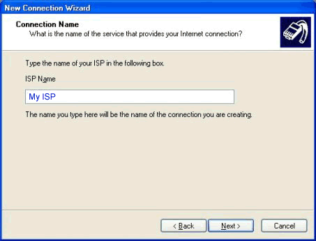
Langkah 8.
- Masukkan nomor telepon ke ISP anda, lalu klik Next.
Langkah 9.
- Tentukan apakah koneksi ini diperbolehkan untuk banyak orang atau anda saja, lalu klik Next.
Langkah 10.
- Isi User name
- Isi Password. Klik pada Confirm password dan ketik lagi.
- Tandai "Use this account name and password when anyone connects to the internet from this computer".
- Tandai "Make this the default Internet connection".
- Tak perlu tandai "Turn on Internet Connection Firewall for this connection".
- Klik Next untuk menuju langkah selanjutnya.
Langkah 11.
- Klik 'Add a shortcut to this connection to my desktop' untuk membuat shortcutnya.
- Klik Finish.
- Selanjutnya bila anda akan menggunakan internet, cukup klik dua kali shortcutnya pada dekstop.
Langganan:
Postingan (Atom)